- About Us
- Products
 Active-HDL NEW
vendor: Aldec
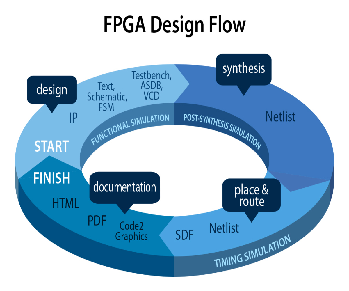
Windows® based, integrated FPGA design creation and simulation solution for team-based environments. LDRAvault NEW
vendor: LDRA
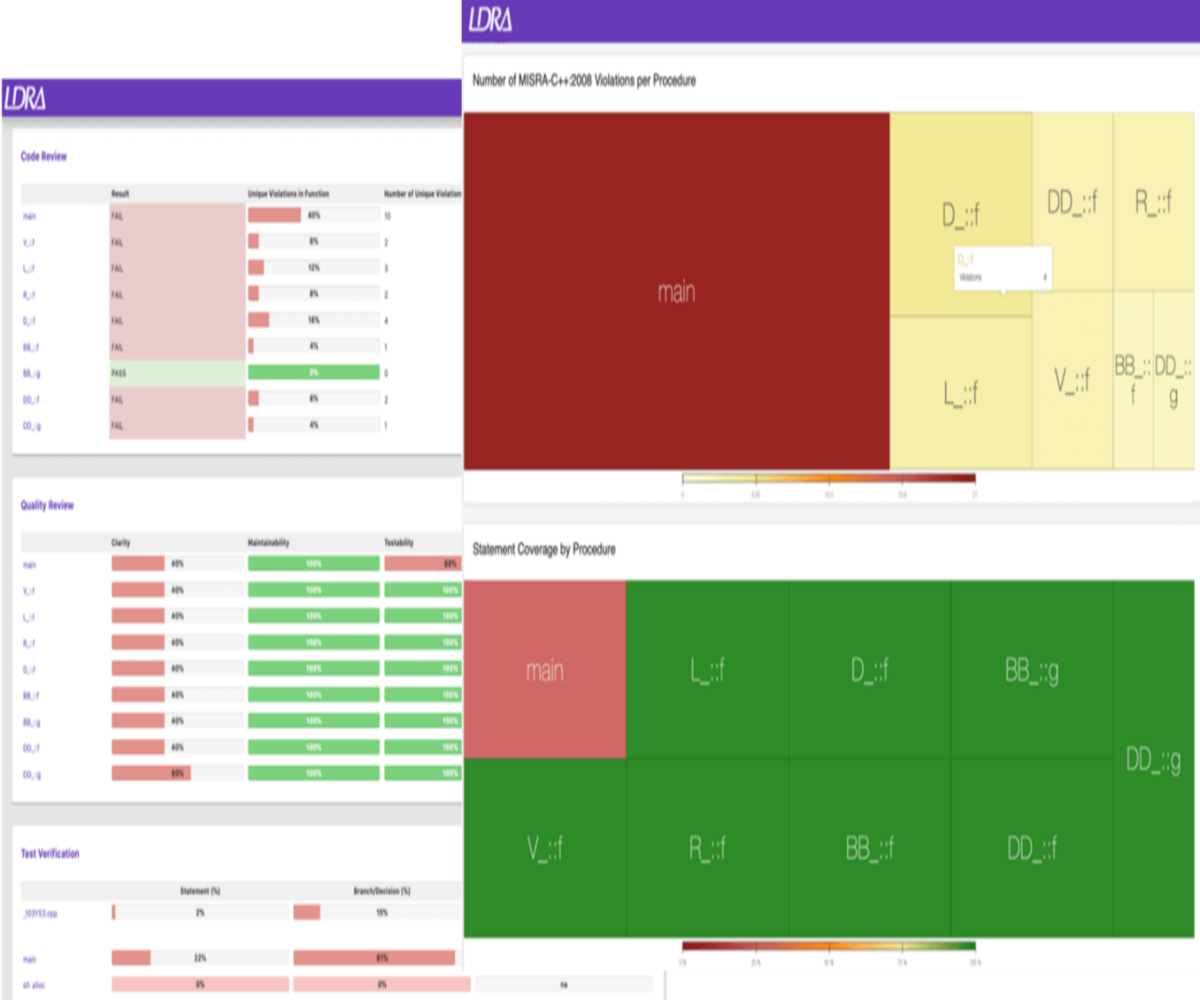
LDRAvault provides a web-interface that automatically aggregates reports and results from the LDRA tool suite. aiT WCET Analyzer NEW
vendor: Absint
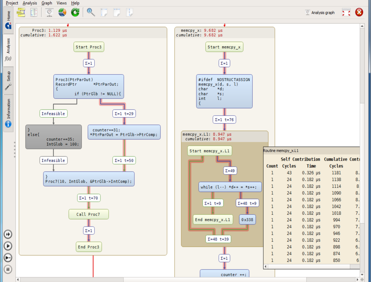
Statically analyze a task’s intrinsic cache and pipeline behavior based on formal cache and pipeline models.aiTWCET Analyzer NEWStatically analyze a task’s intrinsic cache and pipeline behavior…
Qualification SupportLet you simplify and automate the qualification process considerably…
TimeProfilerHelps you identify application parts that cause worst execution time . . .
Active-HDL TOPWindows® based, integrated FPGA design creation and simulation solution…
Alint-PRODesign verification solution for RTL code written in VHDL, Verilog, and SystemVerilog…
DO-254/CTSFully customized hardware and software platform that augments target board testing…
HES NEWFeature-rich family of SoC/ASIC pre-silicon physical prototyping and hardware embedded…
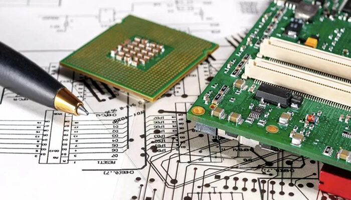
HES-DVMFully automated and scalable hybrid verification environment for SoC and ASIC design…
Riviera-PRO TOPAddresses verification needs of engineers crafting tomorrow’s cutting-edge FPGA…
RTAX-RTSXReprogrammable prototyping solution for Microchip RTAX-S/S and RTSX-SU space-flight…
Spec-TRACERUnified requirements lifecycle management solution designed for FPGA and ASICs…
Jama ConnectImprove quality, reduce rework, prove compliance, and get to market faster
QNX Black Channel CommunicationsA safe software solution for data communications in embedded systems…
QNX HypervisorConsolidate diverse embedded systems with different reliability and security requirements…
QNX Hypervisor for SafetyConsolidate multiple operating systems with different safety requirements on a single system-on-a-chip…
QNX OS for SafetyAn embedded OS pre-certified for IEC 61508 SIL3, ISO 26262 ASIL D and IEC 62304 Class C…
QNX Software Dev Platform 7.1 TOPComprehensive software platform for mission-critical embedded systems…
QNX Software Dev Platform 8.0 NEWFoundational development platform for the next generation…
Safety CertificationsStreamline safety certifications and compliance with embedded software solutions from BlackBerry QNX…
- Services
 Consulting
Edaway provides hardware and software consulting services, that focus on the design and development of a physical product or of software application, including support for V&V activities and for certification aspects.
 Design
Edaway has signed a cooperative agreement with Mindway S.r.l., for providing design services to its customers, in Europe and outside Europe.
 Technical Support
Edaway provides Level 1 technical support to the distributed tools, and the technical interface with the supplier for Level 2 and Level 3 support.
- Partners
- Trainings
 DO-254 NEW
Edaway DO-254 Training covers all aspects of Hardware Considerations in Airborne Systems and Equipment Certification…
 DO-178 NEW
Edaway DO-178C Training covers all aspects of Software Considerations in Airborne Systems and Equipment Certification…
 MISRA C NEW
The MISRA C language subset is a world-leading set of software guidelines, to facilitate code safety, security, portability…
DO-178 TOPEdaway DO-178C Training covers all Software aspects in Airborne Systems…
DO-254 TOPEdaway DO-254 Training covers all Hardware aspects in Airborne Systems…
LDRA Training3-day course provides delegates with a thorough understanding of testing methodologies….
ISO 26262:2018 Compliant SW Dev2-day course focused on the software-related elements of ISO 26262:2018.
ISO 26262:2018 & Automotive Func. Safety1-day course focused on functional safety in the automotive industry in ISO 26262.
MISRA CThe MISRA C language subset is a world-leading set of software guidelines…
QNX TrainingQNX Trainings are focused on features of the QNX® Neutrino® RTOS…
 Ansys Webinar
Leveraging Model Driven Software Development and Automated Software Verification to Deliver Next Generation Avionics Systems.
- Careers
- Contact
- About Us
- Products
 Active-HDL NEW
vendor: Aldec
Windows® based, integrated FPGA design creation and simulation solution for team-based environments. LDRAvault NEW
vendor: LDRA
LDRAvault provides a web-interface that automatically aggregates reports and results from the LDRA tool suite. aiT WCET Analyzer NEW
vendor: Absint
Statically analyze a task’s intrinsic cache and pipeline behavior based on formal cache and pipeline models.aiTWCET Analyzer NEWStatically analyze a task’s intrinsic cache and pipeline behavior…
Qualification SupportLet you simplify and automate the qualification process considerably…
TimeProfilerHelps you identify application parts that cause worst execution time . . .
Active-HDL TOPWindows® based, integrated FPGA design creation and simulation solution…
Alint-PRODesign verification solution for RTL code written in VHDL, Verilog, and SystemVerilog…
DO-254/CTSFully customized hardware and software platform that augments target board testing…
HES NEWFeature-rich family of SoC/ASIC pre-silicon physical prototyping and hardware embedded…
HES-DVMFully automated and scalable hybrid verification environment for SoC and ASIC design…
Riviera-PRO TOPAddresses verification needs of engineers crafting tomorrow’s cutting-edge FPGA…
RTAX-RTSXReprogrammable prototyping solution for Microchip RTAX-S/S and RTSX-SU space-flight…
Spec-TRACERUnified requirements lifecycle management solution designed for FPGA and ASICs…
Jama ConnectImprove quality, reduce rework, prove compliance, and get to market faster
QNX Black Channel CommunicationsA safe software solution for data communications in embedded systems…
QNX HypervisorConsolidate diverse embedded systems with different reliability and security requirements…
QNX Hypervisor for SafetyConsolidate multiple operating systems with different safety requirements on a single system-on-a-chip…
QNX OS for SafetyAn embedded OS pre-certified for IEC 61508 SIL3, ISO 26262 ASIL D and IEC 62304 Class C…
QNX Software Dev Platform 7.1 TOPComprehensive software platform for mission-critical embedded systems…
QNX Software Dev Platform 8.0 NEWFoundational development platform for the next generation…
Safety CertificationsStreamline safety certifications and compliance with embedded software solutions from BlackBerry QNX…
- Services
 Consulting
Edaway provides hardware and software consulting services, that focus on the design and development of a physical product or of software application, including support for V&V activities and for certification aspects.
 Design
Edaway has signed a cooperative agreement with Mindway S.r.l., for providing design services to its customers, in Europe and outside Europe.
 Technical Support
Edaway provides Level 1 technical support to the distributed tools, and the technical interface with the supplier for Level 2 and Level 3 support.
- Partners
- Trainings
 DO-254 NEW
Edaway DO-254 Training covers all aspects of Hardware Considerations in Airborne Systems and Equipment Certification…
 DO-178 NEW
Edaway DO-178C Training covers all aspects of Software Considerations in Airborne Systems and Equipment Certification…
 MISRA C NEW
The MISRA C language subset is a world-leading set of software guidelines, to facilitate code safety, security, portability…
DO-178 TOPEdaway DO-178C Training covers all Software aspects in Airborne Systems…
DO-254 TOPEdaway DO-254 Training covers all Hardware aspects in Airborne Systems…
LDRA Training3-day course provides delegates with a thorough understanding of testing methodologies….
ISO 26262:2018 Compliant SW Dev2-day course focused on the software-related elements of ISO 26262:2018.
ISO 26262:2018 & Automotive Func. Safety1-day course focused on functional safety in the automotive industry in ISO 26262.
MISRA CThe MISRA C language subset is a world-leading set of software guidelines…
QNX TrainingQNX Trainings are focused on features of the QNX® Neutrino® RTOS…
 Ansys Webinar
Leveraging Model Driven Software Development and Automated Software Verification to Deliver Next Generation Avionics Systems.
- Careers
- Contact





![HES_DVM_img[1]](https://www.edaway.com/wp-content/uploads/2024/05/HES_DVM_img1.jpg)
